The Engineering Challenge
To understand the intrinsic transport properties of novel materials, we must move beyond bulk pellets. The challenge lies in making electrical contact with single nanostructures (sub-100nm diameter) without introducing contact resistance or geometric artifacts.
My Mission: To engineer device architectures that isolate the intrinsic physics of the material—whether it is a single perovskite nanorod or a micro-crystal for Hall measurement.
Innovation 1: Single Nanorod FETs (Thesis Work)
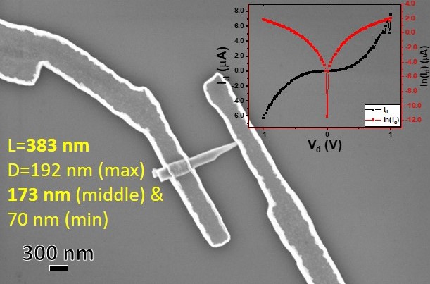
In my doctoral research, I synthesized high-aspect-ratio LaKMnO$_3$ (LKMO) nanorods using a dynamic hydrothermal method. To prove their utility in electronics, I fabricated single-nanorod Field Effect Transistors (FETs).
- Fabrication: 1. Dispersal: Nanorods dispersed on $Si/SiO_2$ (300nm oxide) with alignment markers. 2. EBL Patterning: Used Electron Beam Lithography to define Source/Drain contacts on a single 86nm-radius rod. 3. Result: The device showed p-type semiconductor behavior with an Inverse-‘S’ shaped I-V curve, confirming its potential for neuromorphic computing.
- Key Metric: Calculated carrier mobility ($\mu$) using the transconductance ($g_m$) from the linear region of the $I_d-V_g$ curve.
Innovation 2: The “5-Probe” Hall Architecture
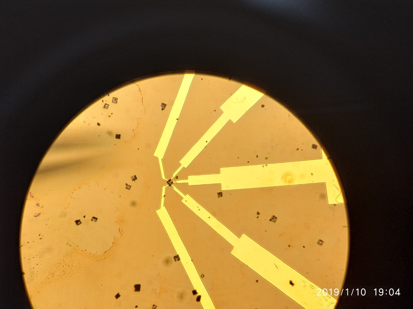
For larger micro-crystals (~15$\mu$m), standard 4-probe methods suffer from voltage mixing ($R_{xx}$ vs $R_{xy}$) due to misalignment. I solved this by engineering a 5-Probe Asymmetric Device using a hybrid workflow.
- Technique: Photolithography + FIB-SEM.
- Process:
- Photolithography: Defined the coarse contact pads and leads on the substrate.
- Focused Ion Beam (FIB): Used Gallium ions to precisely deposit Platinum (Pt) “straps” connecting the specific facets of the microcube to the leads.
- The Logic: The 5th probe (asymmetric arm) allows for the simultaneous decoupling of Longitudinal Resistance ($R_{xx}$) and Hall Voltage ($R_{xy}$), providing artifact-free carrier density data.
Visual Methodology